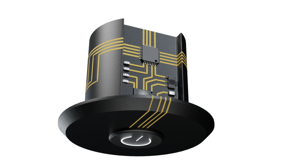
The relentless miniaturization trend in electronics presents a constant challenge: cramming ever-more functionality into ever-shrinking devices. Traditional Printed Circuit Boards (PCBs) are reaching their physical limitations, forcing engineers to seek innovative solutions. The 3D-Circuits technology, which integrates electrical circuits with three-dimensional mechanical parts, offers a promising answer. However, designing these complex structures presented a significant hurdle – a lack of user-friendly design tools.
HARTING, a global leader in connector and interconnect technology with a pioneering spirit in 3D-MID, recognized this challenge. To unlock the full potential of 3D-Circuits, they partnered with Altium, a world-renowned provider of advanced PCB design software. This powerful collaboration resulted in two groundbreaking solutions: Altium Designer’s new 3D-MID design tool and the new HARTING standard product, the PCB Expander.
Seamless 3D-MID Design with Altium Designer
Prior to this collaboration, 3D-Circuits design was a complex and time-consuming process. Engineers often needed specialized software and expertise, hindering widespread adoption of the technology. Altium Designer’s innovative 3D-MID design tool shatters these barriers.
“The collaboration with Altium has been instrumental in making 3D-Circuits design more accessible and efficient than ever before, “says Thomas Hess, Head of PM, Product & Technology Development at HARTING. “This tool empowers engineers to leverage their existing knowledge and workflows, reduces the time for the design and most important, compared to manual layout, it includes electrical design rules and schematic connectivity.

Here’s how Altium Designer streamlines the 3D-Circuits design process:
- Leveraging Existing Assets: Engineers can utilize their standard library components and established schematic designs, eliminating the need to create new components specifically for 3D-MID applications. This saves significant time and effort.
- Intuitive 3D Design Environment: The software provides a user-friendly interface for placing and positioning components directly on the surface of a 3D substrate. This eliminates the need for complex 3D modeling expertise.
- Seamless Connectivity Routing: Connections are routed based on the established schematic logic, ensuring design consistency and reducing errors.
- One-Click Manufacturing Ready: Once the design is complete, a single click generates all the production files required for manufacturing, streamlining the transition from design to production.
Maximizing Space with the HARTING PCB Expander
The HARTING PCB Expander further enhances the space-saving capabilities of the 3D-Circuits technology. This innovative product acts as an extension of the main PCB, eliminating the need for bulky subassemblies and intricate layouts that can eat up valuable real estate.
“The PCB Expander is a game-changer for engineers working in space-constrained environments,” says Michael Mross, Project & Sales Manager at HARTING. “It allows them to pack more functionality into smaller devices without sacrificing performance.”

The PCB Expander offers a multitude of benefits:
- Maximized Space Utilization: By offloading components to the PCB Expander, valuable space/room is freed up on the primary PCB, allowing for the integration of critical functions that would otherwise struggle for space.
- Simplified Design Complexity: The PCB Expander reduces reliance on complex, expensive multi-layer PCB layouts, streamlining the design process and lowering overall costs.
- Seamless Pick-and-Place Integration: The placement of the PCB Expander is designed to integrate seamlessly with standard pick-and-place assembly processes, eliminating the need for additional or specialized manufacturing steps. This translates to faster production times and lower overall manufacturing costs.
- Seamless Design Workflow: The PCB Expander integrates effortlessly with Altium Designer, ensuring a smooth and efficient design experience from concept to production.
Beyond Space Efficiency: A Paradigm Shift in Design
The combined impact of Altium Designer’s 3D-MID design tool and the HARTING 3D-Circuits technology extends far beyond maximizing space utilization. This powerful combination empowers engineers to create innovative and adaptable electronic devices, fostering a paradigm shift towards design efficiency.
“Our partnership with HARTING has allowed us to push the boundaries of PCB design software, “says Jack Henriques, Product Manager at Altium. “The development of the 3D-MID design tool is a testament to our commitment to continuous innovation and supporting the evolving needs of the electronics industry.”
This collaboration unlocks the full potential of 3D-MID technology, paving the way for a new generation of compact, high-performance electronic devices across various industries, from portable electronics and wearables to the Internet of Things (IoT) and beyond.
About Altium
Altium, LLC (ASX:ALU) is a global software company headquartered in San Diego, California, accelerating the pace of innovation through electronics. For over 30 years, Altium has been delivering software that maximizes the productivity of PCB designers and electrical engineers. From individual inventors to multinational corporations, more PCB designers and engineers choose Altium software to design and realize electronics-based products.